

AFM induced nanopatterning of Si surfaces
Y. Zhang, L. Santinacci, T. Djenizian and P. Schmuki
Patterned metal layers are incorporated into integrated circuits for electrical conductivity, junction devices, connection pads, and optical attenuators (in optodevices). These are usu-ally fabricated by depositing the metal (using chemical vapor deposition or electroplating) over the entire surface and then removing the undesired metal by etching the pattern through a mask, by chemical mechanical polishing, by metal evaporation over a patterned resist and lift off or by electroless plating through a mask [1]. For high resolution pattern-ing, most frequently electron-beam, X-ray or ion-beam lithography are used (see, e.g., [2-4]). Other techniques consist of direct patterning such as in-situ modification of surfaces by scanning tunneling microscopy [5]. An alternative approach to achieve ‘‘patterned’’ metal deposition has been presented before [6]. It is based on an electrochemical process, where the ‘‘maskless’’ patterning results from the electrochemical sensitivity to intentionally cre-ated surface defects using focussed ion beam implantation.
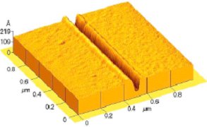
The present work investigates the use of AFM-scratching method on silicon as an approach for selective metal (e.g., Au, Cu and Pd) deposition. The first step of this technique was the introduction of mechanical defects by AFM-scratching onto p- and n-type silicon, see Fig. 1. Single-crystalline diamond coated tips mounted on cantilevers with high spring constant were used in contact mode on a traditional AFM. Well-defined scratches were obtained and protrusions along the sides of the grooves were observed exhibiting a surface deforma-tion induced by the mechanical treatment and indicate the presence of stress. The grooves show a V-shape and their dimensions vary between 7 nm to 40 nm in depth and between 50 nm to 300 nm in width depending on the applied parameters (normal load, number of cycles or scan velocity). Intrinsic properties of the substrate like doping concentration and crystallographic orientation have also an influence on the groove morphology.
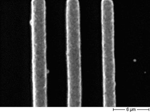
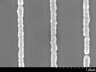
In a second step, metal electrodeposition onto Si surface was carried out by applying a cathodic potential step. Higher reactivity of the scratched area was observed showing that the nano-scratches act as deposition activators. However, total selectivity of the process can only be achieved if scratching is performed through a resist layer present on the surface. The insulating or masking layer can be a thin oxide film (10 nm thick) grown on either a p or n type Si (100) or self-assembled organic monolayer covalently bound to a n-Si (111) surface. Electrochemical techniques are used for Cu deposition in the openings made by scratching through the masking layers. The deposition is carried out either by cathodic potential step deposition or by immersion plating. It is shown that under optimized deposition parameters selective and well-defined metallic structures onto Si surfaces can be produced with a lateral resolution in the several 100 nm range. (Fig.2, 3.).
Parameters like scratch morphology as well as duration and voltage of the potential step used for electrodeposition were studied in this work. The metallic lines were characterized by different microscopies (AFM and SEM) and AES spectroscopy, see Fig. 2. The work therefore demonstrates a new and direct technique for semiconductor patterning and func-tionalization by electrodeposition.
 |
|
| Fig.1 AFM 3D-view of an AFM-scratch in p-type Si (100) performed with a normal load of 14 µN. | |
 |
 |
|
Fig.2: SEM image of copper deposited on 10 nm oxide covered n-Si (100). The scratch was performed by an AFM tip through the oxide layer. The Cu deposition was carried out by a cathodic potential step at –500 mV (vs Ag/AgCl) in CuSO4 (0.1 M) + H2SO4 (0.5 M) electrolyte for 35 s.
|
Fig.3: SEM image of copper deposited on octadecene covered n-Si (111) surface. The scratch was performed by an AFM tip through the organic layer. Cu was electroless deposited in 0.05 M CuSO4 + 1% HF electrolyte for 4 s.
|
References
[1] S. Furukawa and M. Mehregany, Sens. Actuators A, 56 (1996) 261
[2] A. N. Broers, IBM J. Res. Develop., 32 (1988) 502
[3] J. R. Sheats and B. W. Smith, Microlithography: Science and Technology, Marcel Dekker Inc., New York (1998).
[4] P. Rai-Choudhury, Hanbook of Microlithography, Micromachining, and Microfabrica-tion, SPIE Press, Bellingham (1997).
[5] D. M. Kolb, R. Ullmann, and T. Will, Science, 275 (1997) 1097
[6] P. Schmuki and L. E. Erickson, Phys. Rev. Lett., 85 (2000) 2985