

Nanostructured Materials by Selective Surface Activation using Ion implantation
A. Spiegel (EPFL), P. Schmuki (University of Erlangen)
It has been shown before that focused ion beam (FIB) induced damage on p-Si can be used to trigger selective electrochemical reactions [1]. Our research has shown that at semiconductor defect sites the local Schottky barrier breakdown potential is significantly altered when compared to the intact surface. This difference can be used to trigger selective electrochemical reactions at the defect sites only. Hence, maskless metal deposition in the sub-micrometer range becomes possible and may offer new methods for nanostructuring semiconductors [2].
For ion implantation we used the FIB system installed at PSI. We have been working with a Ga ion sources built inhouse. Ions were implanted with an energy of 30 keV and implant fluences were varied over 4 orders of magnitude (1012 - 1016 ions/cm2); the influence of fluence on electrochemical behaviour was investigated. All electrochemical experiments were carried out using a standard three-electrode set-up (sample as working electrode, Pt-counter electrode, standard calomel reference electrode -SCE) under potentiostatic or -dynamic conditions. Different electrolytes were used (0.01 M CuSO4 + 0.05 M H2SO4 (+ 0.1mM BTA) for Cu deposition under varying electrochemical conditions (time, potential, and scanning speed were varied).
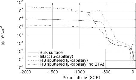 |
Fig. 1: Current-voltage behaviour FIB sensitized p-Si (BTA containing electrolyte)
Using microapillary measurements [3] we were able to show the influence of electrochemical parameters (electrolyte, potential) and the ion implant dose on deposition behaviour. The addition of benzotriazole (BTA) to the electrolyte lead to significantly decreased Cu-crystallite size; it is generally assumed that BTA inhibits crystallite growth by adsorbing to the sample surface where it limits surface diffusion of adsorbed ionic species (in this case Cu++ ions).
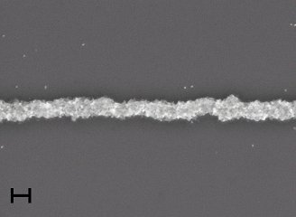 |
Fig. 2: Cu line on p-Si sensitized by FIB (marker is 200nm).
Fig. 2 shows a Cu line deposited on p-Si implanted with ~1·1015 ions/cm2 (20s at –1500mV, electrolyte as before). The electrochemical process visibly reaches the resolution given by the FIB and structures in the sub-micrometer range are easily obtainable. No distinguishable grains or crystallites can be seen in Fig. 2 indicating that even smaller structures are possible. Selectivity is excellent and coverage of the implant site is complete.
In the near future we will focus our attention on further optimizing the deposition procedure and we are confident to reach the sub 100nm-resolution soon. Also, more fundamental aspects of the electrochemical behaviour will be investigated.
References
[1] H. Böhni, T. Suter, and F. Assi, "Micro-electrochemical techniques for studies of localized processes on metal surfaces in the nanometer range", Surface and Coatings Tech-nology, 130 (2000) 80
[2] P. Schmuki, L. E. Erickson, and D. J. Lockwood, "Light emitting micropatterns of porous Si created at surface defects", Phys. Rev. Lett., 80 (1998) 4060
[3] A. Spiegel, L. E. Erickson, and P. Schmuki, "Selective growth of porous silicon on focused ion beam patterns", J. Electrochem. Soc., 147 (2000) 2993