
Sensitization of semiconductor surfaces for totally selective electrochemical reactions
P. Schmuki
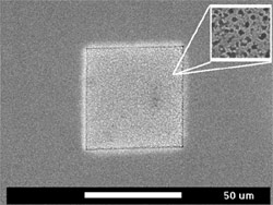
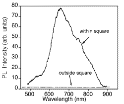
In a collaboration with the National Research Council of Canada it has has shown that red light emitting porous Si can be produced at defined surface locations of a Si substrate by a direct writing process using focused ion beam technology combined with electrochemistry [1].
The principle is that the growth of porous Si growth can electrochemically be initiated preferentially at surface defects created in a single crystal Si substrate by ion bombardment. Using a focused ion beam (FIB) as a source of ions, arbitrary defect patterns in the 50 to 200 nm range can be written into a substrate. The selectivity of the subsequent electrochemical dissolution reaction seems to be due to a facilitated Schottky barrier breakdown at the implanted surface defects which leads to the desired "localized current flow".
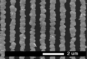
In more general terms this preliminary work shows the feasibility of a new principle for locally activating or sensitizing a semiconductor surface for a subsequent chemical or electrochemical reaction. This principle is not only applicable to trigger the growth of po-rous Si structures on pre-defined and confined surface locations but can also be exploited for highly localized direct electrochemical deposition reactions [2]. This provides the basis for much wider applications in surface physics, chemistry and materials science, as depo-sition of all materials that currently can be electrodeposited on a larger scale (metals, other semiconductors or ceramics) should be possible in a submicron scale.
Further work will investigate this local porous semiconductor formation mechanism in detail (including recently discovered light emitting porous GaAs [3,4]). On the other hand, key factors and perspectives of local electrodeposition processes will be studied.
|
||||||
 |
||||||
| Selective Au deposition on Si sensitized with FIB lines |
References:
[1] P. Schmuki, L.E. Erickson, D.J. Lockwood: "Light Emitting Micropatterns of
Porous Si Created at Surface Defects", Phys. Rev. Lett. 80 (1998) 4060
[2] P. Schmuki, L.E. Erickson,: ”Selective deposition of metal nano-patterns on
silicon” , Phys. Rev Lett. , 85 (2000) 2985
[3] P.Schmuki, D.J. Lockwood, H.J. Labbe, J.W. Fraser: "Visible
Photoluminescence from Porous GaAs", Appl. Phys. Lett. 69 (1996) 1620
[4] P. Schmuki, L.E. Erickson, D.J. Lockwood, J.W. Fraser, G. Champion, H.J.Labbe:
"Formation of visible light emitting porous GaAs micropatterns", Appl. Phys. Lett. 72 (1998) 1039
| Click on the PDF icon to download this page |