

Self organized InP nanotubes/nanopores by anodization
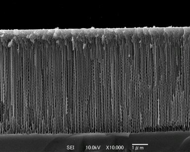
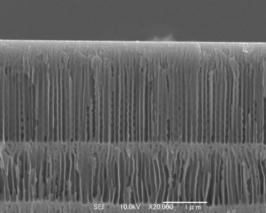
The localized dissolution of semiconductors has generated a great deal of interest since discovery of efficient visible photoluminescence in porous Si. For III-V compound semiconductors such as InP, resulting porous layers are strongly affected by electrochemical conditions used. For low currents or potentials anodization, porous layers with a facet-like structure are formed. For high currents or potentials, a tree-like structure with random and/or tangle branches is formed(Fig. 1). Under optimized conditions, the porous layer exhibits fairly regular arrays of straight pores(Fig. 2). By changing the applied current/potential periodically, highly defined and ordered superlattices consisted of a stack of two layers with alternating high and low porosity are formed on n-type (100) InP surface. This structure is applied for waveguides, distributed Bragg reflectors and bio-chemical sensors.
 |
 |
|
| Fig. 1 SEM image of the highly ordered straight porous structure. | Fig. 2 Cross-sectional SEM image of the porous superlattice sample anodized by changing applied currents periodically. |