

Self-Assembled Monolayers as resist layers for patterning of Si (111) surfaces.
E. Balaur, T. Djenizian, Y. Zhang, P. Schmuki
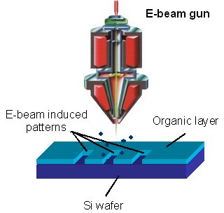
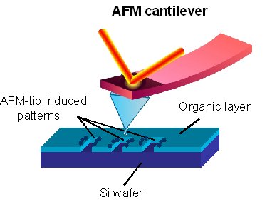
The interest in the general area of self-assembled monolayers (SAM) stays partially from their perceived significance to science and technology. Chemical functionalization of materials surfaces has many potential applications ranging from surface passivation and stabilization to development of new strategies for immobilization of either chemical or biological species on the surface and detection of diverse interactions characterizing biological and chemical systems. Due to their typical thickness of 1-2 nm, SAMs can be used as novel resists that permit high-resolution patterning. SAMs were successfully utilized as positive and negative resist on Si(111) surfaces for nanostructure fabrication by electron beam technique (Fig.3) and also by AFM lithography (Fig.4).
 |
 |
|
Fig. 1 E-beam induced modification of SAMs
|
Fig. 2 AFM-tip induced modification of SAMs |
 |
 |
|
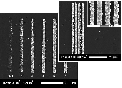
Fig. 3 SEM image of a sample carrying the Cu lines pattern previously described in Fig.1 after a potentiostatic experiment consisting of applying a cathodic potential (-350 mV vs (Ag/AgCl)) for 300 s
|
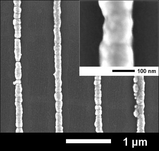
Fig. 4 SEM image of a sample carrying the Cu lines pattern previously described in Fig.2 after an immersion deposition during 15 sec |