

Nanostructuring of electrode surfaces with an electrochemical STM
Y. Zhang, S. Maupai, P. Schmuki
With an electrochemical Scanning Tunneling Microscope (EC-STM) it is possible to ob-serve and modify electrode surfaces under potential control on a nanoscale [1]. One ap-proach to understand nucleation and growth in homo- or heteroepitaxy is to follow the ini-tial steps of electrochemical metal deposition on the surface [2].
In some electrochemical systems the first step of metal deposition is the so called underpo-tential deposition, that is the formation of one atomic layer of metal to be deposited on a foreign substrate. In the case of Cd-deposition on Au(111) the deposition of such a monolayer starts at about 350 mV positive of the reversible Nernst-potential for Cd-bulk deposition [3].
When a flame annealed Au(111)-surface is used as a substrate, the Au-surface is recon-structed and shows the typical “herringbone”-structure of parallel corrugation rows due to a contraction of the upmost atomic layer for about 4 %. By observing the initial nucleation of Cd on this surface we found, that the angles of the reconstruction rows are the sites of preferred nucleation (Fig. 1a, b). The well defined distance between the reconstruction rows can therefore be used to cover the hole surface in a self-assembling way with Cd clus-ters that consist just of a few atoms (Fig. 1c). Alternatively potential induced reconstructed Au(111) surface. The potential induced reconstruction normally does not lead to large-scale herringbone zigzag patterning but moreover to irregular and random reconstructed morphologies. As we can see from Fig 2.
The Cd nucleation in the underpotential regime proceeds exclusively based on the elbow sites of the Au(111) herringbone reconstruction leading to a self organized surface patterning consisting of nanoscale Cd islands and lines. The coverage of the surface with nuclei can be controlled at any stage by applying the appropriate potential.
The next step of this work will be to emerge the cluster covered surface from the electro-lyte under potential control and transform the Cd clusters chemically into CdS clusters. The CdS clusters of such size should exhibit real quantum confinement effects that will be measured as photoluminescence for example.
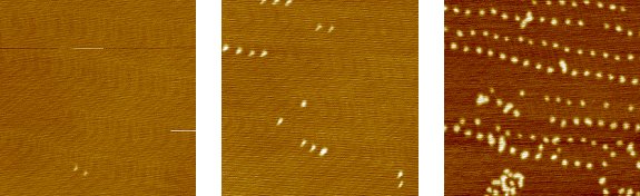
Fig. 1: (100 nm x 100 nm) Au(111) in 0.05 M H2SO4 / 0.5 mM CdSO4, a) E = 330 mV vs. Cd/Cd2+, b) E = 260 mV vs Cd/Cd2+, c) E = 220 mV vs. Cd/Cd2+
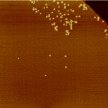
Fig 2. (200 nm x 200 nm) Au(111) in 0.05 M H2SO4 / 0.5 mM CdSO4, at 200 mV vs. Cd/Cd 2+
References:
[1] S. Maupai, M. Stratmann, A.S. Dakkouri, Ex Situ Characterization of Electrochemi-
caly Generated Cu Nanostructures, Electrochem. Sol. State Lett., 5 (2002) C35
[2] R.J. Randler, D.M. Kolb, B.M. Ocko, I.K. Robinson, Electrochemical copper deposi-
tion on Au(100): a combined in situ STM and in situ surface X-ray diffraction study,
Surf. Sci., 446 (2000) 187
[3] R. Vidu, S. Hara, In Situ EC-AFM Observation of Cd Electrodeposition on Au(100),
Scripta Mat., 41 (1999) 617