

Electron-beam induced nanomasking for metal electrodeposition on semiconductor surfaces.
T. Djenizian, L. Santinacci, P. Schmuki
Lithography using beams of electrons is one of the most employed approach used for inte-grated circuit fabrication. In technological applications electron beam (e-beam) systems play two vital roles: they are used to fabricate masks for optical exposure systems (as well as x-rays systems) and create ultrasmall features for very high performance devices. The principle is mainly based on the exposure of resists (e.g. PMMA) to e-beam. In research, however, exploratory of direct processes have been investigated to generate ultrasmall linewidths on semiconductor surfaces as well as to create 3D nanostructures in the nm range using e-beam induced deposition (EBID) reactions [1-3]. In this approach, the e-beam activates gaseous precursor species introduced into the vacuum chamber of the e-beam instrument leading to a solid deposit at the irradiated surface and consequently a cone of resist builds up at the point of impact of the e-beam. Typically the precursor vapor species used for EBID are metallorganic compounds.
The residual hydrocarbons issued from the pump oil can also be used as precursors species. It has been widely reported that deposition of carbon occurs in vacuum systems pumped with untrapped oil diffusion pumps. Indeed this contamination resist is formed when the e-beam “cracks” the thin layer of hydrocarbon molecules condensed at the sample surface. In that case, the hydrocarbon molecules adsorbed on the surface react under e-beam to form an amorphous structure of carbon, more specifically a layer of diamond-like carbon (DLC). Such contamination writing has been successfully applied as a mask using ion milling [4] or to fabricate devices like microbridge SQUIDs [5]. Recently this technique has been used to achieve high definition patterning of semiconductor surfaces for subsequent metal elec-trodeposition [6-8]. In this work it has been showed how to use C-masks produced by con-tamination writing in a SEM to suppress completely and selectively metal electrodeposi-tion at treated surface locations.
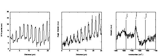
In order to study in details e-beam induced carbon deposition reactions, a series of ten lines was deposited using different electron doses in a JEOL 6400 SEM. Subsequently, the lines were analysed by various techniques including AFM, AES and Raman spectroscopy (Fig. 1).
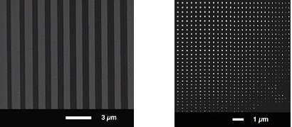
Due to the predominant amount of C sp3, it has been demonstrated that such carbonaceous deposits in the order of only few nm in thickness can be sufficient to achieve a negative resist effect [6,7]. Figure 2a shows a SEM image of a sample carrying the C-line pattern previously described after a potentiostatic experiment consisting of applying a cathodic potential (-1.8 V vs (Ag/AgCl)) for 30 s. From this picture it is apparent that the surface is entirely covered by a Au deposit except for lines that correspond to the location of the carbon lines. Therefore it is evident that C-deposit acts as a mask for the electrodeposition of metal and constitutes a negative resist if a sufficient contamination layer is present. In order to explore the lower size limit of the deposition process, a series of experiments was performed by minimizing the distance between parallel C-lines. Figure 2b shows an exam-ple of the best resolution attained so far where two arrays of perpendicular C-lines were produced under a 5 kV e-beam. The space between lines is reduced from the left to the right and from the top to the bottom. C-deposits lead to confined Au clusters with the smallest size in the order of 30 nm.
Recently, this technique has also been successfully used to produce selective CdS on sili-con [8] and to fabricate porous silicon [9,10] opening new perspectives for the patterning of surfaces of a wide large palette of materials in the sub-100 nm range.
 |
|
Fig. 1.: AFM profile of 10 C-deposits produced under a 5 kV e-beam for increasing electron dose exposures from the left to the right (a), AES line scan for C across the lines (b) and typical Raman spectrum of the C-deposits (c).
|
 |
|
Fig. 2.: SEM image of a sample carrying the C-line pattern previously described in Fig.1 after a potentiostatic experiment consisting of applying a cathodic potential (-1.6 V vs (Ag/AgCl)) for 10 s (a). Fabrication of Au clusters by decreasing the space between two arrays of perpendicular C-lines (b).
|
References:
[1] H. W. P. Koops, J. Kretz, M. Rudolph, M. Weber, G. Dahm, and K. L. Lee, Jpn. J. Appl. Phys., 33, Part 1, 12B, (1994) 7099
[2] M. Komuro, and Hiroshima, Microelectronic engineering, 35 (1997) 273
[3] N. Miura, H. Ishii, J. Shirakashi, A. Yamada, and M. Konagai, Applied Surface Sci-ence, 113/114 (1997) 269
[4] A. N. Broers, W. W. Molzen, J. J. Cuomo, and D. Wittels, Appl. Phys. Lett., 29 (1976) 596
[5] P. Chaudari, A. N. Broers, C. C. Chi, R. B. Laibowitz, E. Spiller, and J. Viggiano, Phys. Rev. Lett., 45 (1980) 930
[6] T. Djenizian, L. Santinacci, and P. Schmuki, Appl. Phys. Lett., 78 (2001) 2940
[7] T. Djenizian, L. Santinacci, and P. Schmuki, J. Electrochem. Soc., 148 (2001) 197
[8] T. Djenizian, B. Petite, L. Santinacci, and P. Schmuki, Electrochim. Acta, 47 (2001) 891
[9] T. Djenizian, L. Santinacci, and P. Schmuki, Surf. Sci., submitted (2001).
[10] T. Djenizian, L. Santinacci, and P. Schmuki, Appl. Phys. Lett., submitted (2001).