
Surface Analysis and Microscopy
At LKO, a broad range of equipment for surface characterization is available. The chemical composition of surfaces can be studied by Auger Electron Spectroscopy or by X-Ray Photoelectron Spectroscopy.
The AES equipment enables also measurements of the surface composition with a high lateral resolution (~ 50 nm)
(Scanning Auger Microscope: SAM). The surface morphology will be studied by a high-resolution Field-Emission Scanning Electron Microscope including Energy Dispersive X-ray Spectroscopy and Electron Backscatter Diffraction - EBSD, EDAX/TSL. For investigations of the crystal structure, an X-Ray Diffractometer (XRD) thin-film XRD is available. Further, Atomic Force Microscope (AFM), Scanning Tunnel Microscope (STM), Fourier Transformed Infrared Spectroscope (FT-IR), Ellipsometry and Scanning Electron Microscope with e-beam lithography are provided.
A high number of electrochemical work stations (including high-voltage potentiostats for anodizing and impedance spectroscopy) are available for the project. A photoelectrochemical set-up will be used for the characterization of the semiconducting properties. A Rapid Thermal Annealing (RTA) system will be used for annealing of the anodized samples. Microelectrochemical setup (Microcell System) based on the glass capillary technique is used to measure local electrochemical changes of specific surface sites with a local resolution in the µm-range.
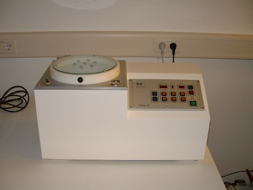
Latest in the line of equipment for surface characterization and analysis at LKO is Time-of-Flight secondary ion mass spectrometer (TOF-SIMS), which provides detailed elemental and molecular information about surface, thin layers, interfaces of the sample, and gives a full three-dimensional analysis.
| Time-of-Flight secondary ion mass spectrometer (TOF-SIMS, ION-TOF GmbH - TOF.SIMS 5) |
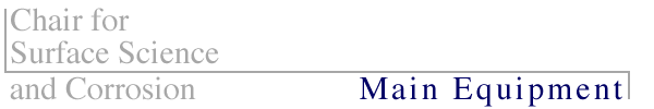
| Auger Electron Spectroscopy (AES, Physical Electronics 670) |
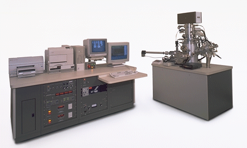
| X-Ray Photoelectron Spectroscopy (XPS, Physical Electronics 5600) |
| High-resolution Field-Emission Scanning Electron Microscope (FE-SEM, Hitachi S4800) |
| Energy Dispersive X-ray Spectroscopy (EDX, EDAX/TSL Genesis 4000) |
| Electron Backscatter Diffraction (EBSD, EDAX/TSL Pegasus 2200) |
| X-Ray Diffractometer (XRD, Philips X'Pert) |
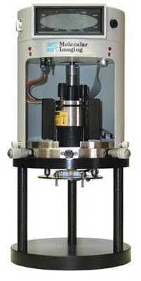
| Atomic Force Microscope (AFM, PicoSPM / Nanoscope E) |
| Scanning Tunnel Microscope (STM, PicoSPM / Nanoscope E) |
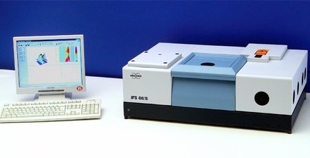
| Fourier Transformed Infrared Spectroscope (FT-IR, Bruker IFS 66/S) |
| Ellipsometry (Sentech SE 800) |
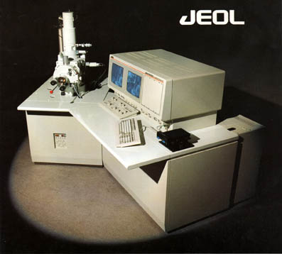
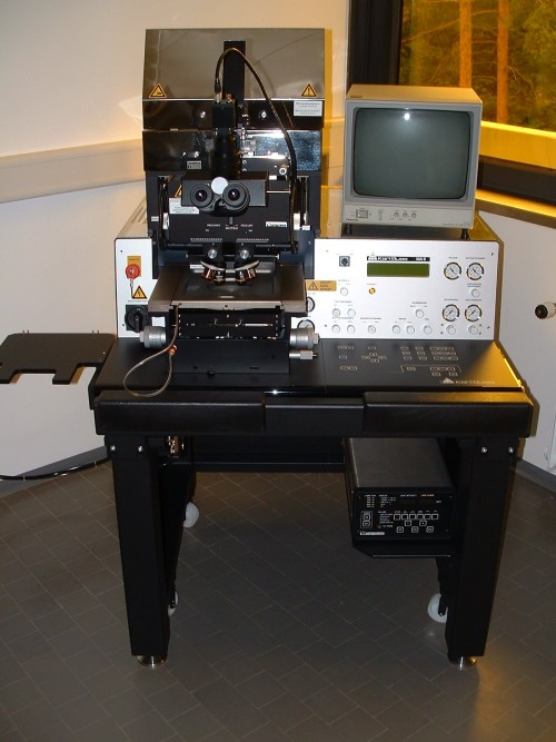
| Scanning Electron Microscope (Jeol JSM 6400) |
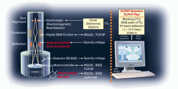
| E-beam lithography (Raith Quantum) |
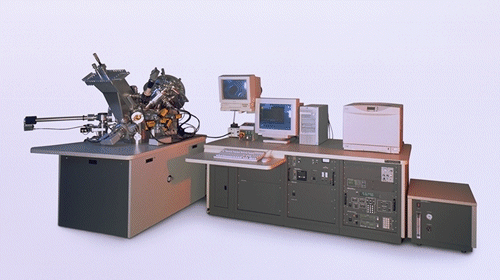
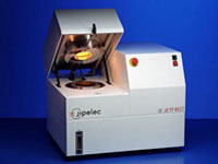
| Rapid Thermal Annealing (RTA, Jipelec JetFirst 100) |
| Microelectrochemical setup (Swiss Microcell System) |
Scanning Probe Techniques
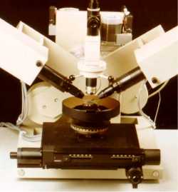
STM/AFM (non-contact) / friction microscopy in air and in electrolytes
STM/AFM for electrochemical investigations
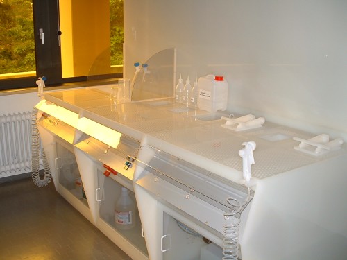
Gray-room
:
Mask aligner
Spin coater
Wet bench
(photolithography and metal or oxide etching)
Optical Microscope
Electrochemical Characterization
Potentiodynamic and potentiostatic methods (Jaissle)
Electrochemical impedance spectroscopy (Zahner IM6 / IM6ex)
High Temperature Oxidation
Furnaces using:
Thermogravimetry
Volumetry
Thin film evaporator
Electron-beam sputtering
Thermal evaporation
Magnetron-sputtering
Materials Testing
Temperature-humidity chambers
Salt-spray chamber
Stress Corrosion Cracking Testing